Simple High Impedance Probe
Motivation
For many measurements, a passive oscilloscope probe is not suitable.
The 10 Megaohms input resistance of passive 10:1 probes may influence high impedance circuits.
At higher frequencies the capacitance of approx. 15pF is problematic: Yet at 20MHz the impedance is only 530 Ohms.
First, this loads the target circuit, second, this load current has to flow back through the ground lead. Without a very low impedance ground connection there will be heavy ringing.
Commercial FET probes are available with input capacitances of less than 1pF and bandwiths >1GHz, but they are pretty expensive and have a very limited voltage range.
A simple circuit will be sufficient most times and has other advantages, e.g. wide voltage range.
Circuit
The schematic in an example configuration:

It has to be connected via coax cable to a correctly terminated scope input.
T2 is the source follower with a typical G-D-capacitance of 1pF. By soldering the gate lead directly to the circuit (why not?), this is the effective capacitance of the probe! That's as good as many commercial products. You likely will have some spare FETs, so you don't need to worry about accidental destruction.
T1 and P1 are the bias current source. P1 has to be adjusted to achieve 0V G-S-Voltage at T2 (zero adjust). Due to tolerances, there is a slight probability that a BF245B is weaker than the BF245A and you can't adjust to zero. In this case, throw it away or swap both. Or use a BF245C for the current source.
The components around the amplifier can set amplification or attenuation as you need.
For signal amplitudes >1V a 10:1 attenuation is suitable, since you want to drive 50 Ohms and the output current of the amplifier is limited. You can attenuate in front of the amplifier (R1, R2) and/or behind it (R4 against the 50 Ohms), depending in the amplifier: much input capacitance => low R1, low slew rate => attenuation in front of the amplifier.
Pay attention not to load the FET too much, I wouldn't draw more than half the quiescent current. And consider the charging current for the amplifier's input capacitance, e.g. 1V/ns, 1pF yields 1mA!
For low signal amplitudes a 1:1 version is suitable. Since most amplifiers don't like to drive cables directly, you will need some amplification before the cable, e.g. R3 = R5 (G = 2) and R4 = 50Ohm.
Some amplifiers want to have R3 und C1 even when used as follower (e.g. 200Ohm, 3,9pF for the THS4001).
The supply decoupling depends on the amplifier needs. The Tantalum capacitors C11, C13 may be smaller than showed. R10, R11 are optional to avoid resonances with the supply leads. When needed, chip ferrites or resistance values of approx. 10 Ohms can be used.
Test results
I built the probes with a THS4001, with 270MHz bandwidth but "only" 0,4V/ns slew rate. Therefore I selected an attenuation of 6,66 kOhms : 1 kOhms in front of the amplifier and a cable series resistor of only 15 Ohms. The typical 1,5 pF of the THS4001 result in 100MHz theoretical bandwidth with the 870Ohm source impedance of the divider, according to 3ns rise time. Since I don't need all the bandwidth, I use a leaded 1 kOhms resistor as probe tip (see pictures below), avoiding catastrophic current flow. With this resistor I measured a bandwidth of 60 MHz as expected.
The BF245 should be much faster, with an appropriate amplifier I expect bandwidths of >100MHz.
I also tested a LM6171 (thanks to Rolf Bombach!) because this one has a much higher slew rate of 3,6V/ns, therefore I used it as follower and set the 10:1 attenuation with a 450 Ohms output resistor, but the LM6171 seems to be undercompensated and rings for approx. 20ns after fast transients. Maybe this can be optimized, but I'm happy with the THS4001.
Construction
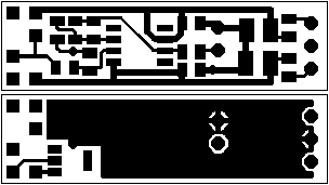
I made a 36mm x 10mm "large" PCB (not larger than a passive probe), being sufficiently robust when put into a piece of shrink tube:


Soldering the probe tips directly into the circuit is fast and more robust than any kind of clips.
Here is the layout of the board:

Power supply:
The FETs should have at least 5V headroom. That's also enough for the amplifier.
For 5V logic levels, I use -5V, +10V supplies. The probe should work at 30V total supply voltage, I often measure 15V levels (with -5V and +20V supplies).
Possible improvements
The circuit has a bad DC precision, not least due to thermal effects, because the power in T1 and T2 depends on the input voltage, therefore their temperature and the offset voltage. After a voltage step, one can observe a thermal tail. This gets worse with higher bias currents (BF245B).
A DC feedback loop can compensate this.
Status
This article is based on a Usenet discussion in the de.sci.electronics news group dated 2000-11. The first release was 2002.
Today (2013), the through-hole BF245 are obsolete, but there are on-hand inventories.
- Oliver Betz - Neuried / München
- Impressum
- Datenschutz